Rationale
Digital hardware development is my hobby. I remember the time I met the microcontroller technology at the university and how impressed I was by the fact that many hardware-related tasks could be solved by just writing some code (which was my main specialization). At that time it was Atmel 51 architecture microcontroller, but soon I switched to AT90 series. The very first device i built had no RAM, only 32 8-bits registers and almost no peripheral except IO pins. Most of the chips available for enthusiasts required special programming devices to upload firmware and expensive hardware emulators to trace and debug. Oh good old (full of pain) times... Nowadays a microcontroller that costs a few dollars has 100-200Kbytes of RAM, several SPI/UART and analog interfaces, more than 100Mhz core frequency and JTAG debugging interface onboard.
At some point of my life i decided to leave my hometown and start travelling. A lot of stuff like oscilloscopes, soldering station, parts boxes i had to leave taking my portable oscilloscope and a soldering iron only. That happened in 2019 and since then i struggled with prototype and evaluation boards each time i wanted to do something hardware related. All that wires, unstable contacts... and all the efforts could get multiplied by zero with a single tail move of my cat... Bruh!
Another problem i encountered during my hobby 'career' is that when you build rare (like i do) you need to start from scratch every time you need to build something trivial and that's pretty much time consuming. You need to install some IDE, find and read some datasheets to refresh some details like IO bus power configuration and core clock options... and finally find the boards to program. I wish i had had a better development approach that would avoid this low-level stuff when i needed to build something simple. In the end of the day, I'm a software developer and the software is the only thing i work on every day and i would have been happy to utilize this knowledge for the hardware too.
The motorcycle breakdown was the turning point. Contemporary vehicles are full of electronic sensors to explore and test, 2-channel oscilloscope was not enough anymore so i decided to build something for that case, something that could read a wide range of electrical signals, record them, process and provide some electrical outputs in real time.
So, the aim was: when i needed a particular device, i wanted to use soldering as little as possible but at the same time avoid jumper wires, reuse existing parts form the previous uses and avoid firmware development when possible. And wanted to have everything packed in a small firm case protecting the scheme during long term storage or outdoor use. And cat proof.
Requirements
As I said, I wanted the device to cover as many applications as possible, it needed to be able to be adjusted for future uses without total rebuilding. I was building rather a convenient playground than a finished device. A good start here would be the requirements and affordable limits.
What I thought was useful and important for my case:
- first of all, as it was intended to interact with other devices/sensors, it needed to have a number of external connectors;
- ability to read and generate discrete and analog signals of different levels (3.3V, 5V, 12V, and more);
- ability to process signals close to real-time as some applications require fast response with guaranteed predictable latency;
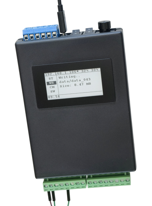
- a screen so it could display some basic info about its state and measurements without attaching to a PC or smartphone;
- also some controls like buttons to interact with the operator;
- needed to be small enough, something near a portable oscilloscope or multimeter in size;
- ability to store information (like signal logs) on an SD card;
- protected inputs and outputs: everything that connects to the external environment should be protected with intermediate buffers so any unexpected signal on any input or unpredicted output load damages the easy-to-replace and cheap buffer components;
- USB-powered: nowadays USB sockets can be found anywhere, and being able to be powered with USB 5V is a big advantage;
There were some additional requirements I wanted to satisfy:
- I wanted to be able to change the schematics without any special equipment: replace the components, change the interconnections;
- at least some discrete outputs needed to be powerful with the ability to switch 20A+ current continuously;
- I expected some applications to require additional components I didn't think about at the time of development, so I wanted to have some free space on the PCB with free pads and footprints: popular component placeholders like resistors, transistors, and amplifiers;
- I thought it would be nice to have the connectors detachable, so I could plug and unplug the device on demand without "re-wiring";
- some additional equipment like relays would be nice to have onboard;
There were some things I intentionally decided to avoid:
- uncommon wireless technologies like LoRa transmitters and GPS receivers - because of different customs rules in different countries;
- integrated power supply battery - it's much easier to connect a rarely used device to a power bank than to spend precious internal space for a battery and charging circuits;
Implementation
The requirements above brought me to the next device scheme:
The core idea here was to have 2 parts combined in one device:
- real-time STM32 microcontroller device that reads inputs and provides output signals in real time (or close to real time). This part, running at up to 168MHz, performs precise pulse width measurements, converts analog signals at 2 MS/s, and generates analog signals of arbitrary form;
- powerful (in terms of development environment) Raspberry Pi Zero 2W part, which is responsible for configuring the STM32 part of the device, reading data from RT, writing files, Wi-Fi/Bluetooth communication, SSH connection, and everything else that little boards provides.
As for the human interface, I decided to go with a small e-paper screen with integrated touch sensor. The main reason was that I used this one in some other Raspberry Pi projects (including my little home server) and had some experience and ready-to-use software. It has an integrated capacitive touch screen (connected via I2C interface to RPi) and e-ink technology is good for outdoor use under bright sun. The resolution is small but enough to provide some basic information about current device configuration and measured signals.
Input and output buffers are some elementary schematics to protect STM32 (and RPI) from "aggressive" external environment like high voltages or positive/negative voltage spikes produced by inductive loads, etc. And from incorrect connections. For discrete signals, the buffers are just small MOSFETs; for analog - operational amplifiers. That is.
One may find the design peculiar and ask why Raspberry PI is used while STM32 can handle all the tasks alone running a RTOS? The answer is simple: i don't have wide experience with any RTOS and acquiring such knowledge is not in the nearest plans. I wanted to use the device in a convenient way for me: log into using SSH, run services in the way i used to, fix bugs using the standard tools i know and love (vim, tmux, gdb). Learning new stuff is cool but what you don't use often you forget it... The opposite question may be asked: why not stick to Raspberry PI - it has general purpose inputs and outputs onboard? True, it has. But it was enough for most applications I was thinking about. Like, it has no ADC or DAC, limited external interrupt abilities, and even if you go to kernel level to write some logic - still no latency guarantees because of the OS type used. Sometimes fractions of microsecond matter.
Ideally, I would like to have the STM32 part to have as flexible firmware as possible so the most use cases would require me to write code for the Raspberry Pi part only in C++ or Python. So STM32 would act as a device (/dev/ctlpie) for the Linux-based RPi.
PCB
The size of the board is 90mm x 110mm. Here is the bottom side (where the STM32 microcontroller is supposed to be soldered on):
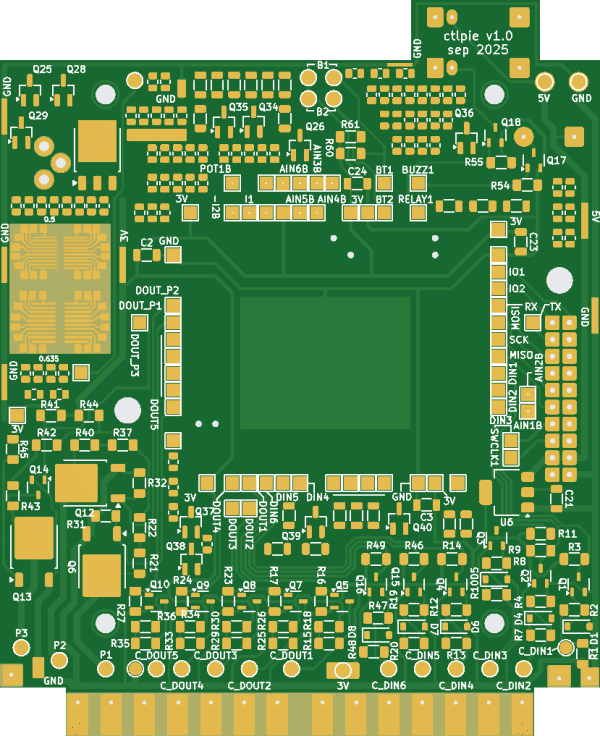
The area at the bottom is filled with repeating patterns of similar discrete input and output buffers (small MOSFET buffers) and 3 powerful open-drain outputs at the left. Each buffer has soldering pads for additional components like Zener diodes and pull-up resistors. These components are not mandatory but have reserved installation places just in case for some applications.
Input and output buffers are not traced directly to the connector socket; they are supposed to be soldered on demand, implementing input and output types set appropriately for the moment. For example, during my motorcycle repair, I used 10 inputs (discrete and analog) but only one output (powerful MOSFET to control the fuel injector).
Buffers are not soldered directly to the microcontroller either. I wanted to be able to change this schematic too. Sometimes I need analog buffers to be connected to ADC inputs of the microcontroller and measure signal levels and waveform. Later, I will reconfigure the analog buffers to act as discrete comparators, and that will require the buffer to be connected to the microcontroller accordingly.
There are many untraced pads and footprints at the top and left, those for future design. Not sure if it is the best way to extend the features of the board, but it's better than nothing. Doesn't hurt.
I used STM32F407 in the LQFP-100 package but decided to avoid soldering it directly on the board and used the adapter for convenient rewiring:
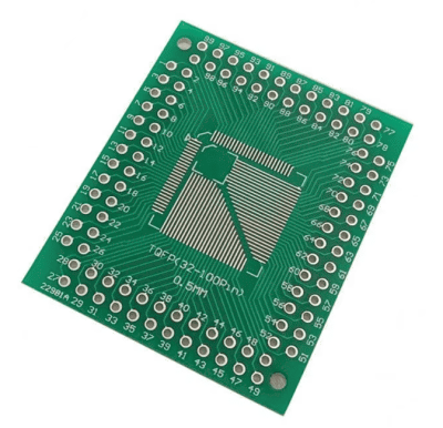
Soldering connection wires to the adapter takes time but pays off - during the first use I rewired some microcontroller outputs several times. And I will rewire in the future for sure. The adapter footprint could have been printed on the board directly, and that could save much time during assembly, but in this case, changing the microcontroller would require a hot air station. With a separate adapter, I can just cut off the connections wire by wire and then just replace the chip together with the adapter.
The PCB is designed to be mounted on the bottom part of the plastic case. A 20-pin connector footprint at the right is for connection to the top part of the case where the Raspberry Pi 2W and e-paper screen are mounted. Both parts share a common 5V power line.
Top layer of the board is for the analog part of the device. It contains analog buffers, footprints for additional analog chips, and uses a separate ground and power supply line including a linear 3.3V stabilizer. Every output buffer amplifier is connected to the power line via a zero-ohm resistor. In case higher output voltage is required, the resistor is to be removed and replaced with a wire to the source of the desired voltage. Each analog buffer has an input voltage divider to adjust higher input voltages to the 3.3V range and adjustable-gain schematics to do the opposite task. Every analog input buffer may be used in the reverse direction (becoming an output buffer) when needed.
As for the controls, the PCB has the pads for 2 switchers or buttons and two potentiometers (one regular and one precise). I thought that would be enough as the device had a touchscreen.
First usage experience
The very same day the assembling was finished i connected the device to my motorcycle ECU. The vehicle was struggling to reach 7k RPM while had been able to run at 10k before. Before the engine disassembling i wanted to be sure that it was not an electrical problem. The motor had EFI system with a wide range of sensors:
- crankshaft position sensor (CKP) producing sin wave signal with a missing period as a sync point;
- manifold absolute pressure sensor (MAP) measuring the vacuum in the intake manifold;
- oxygen sensor in the exhaust line;
- engine temperature;
- throttle position sensor (TPS);
- intake temperature sensor (that one i ignored as it was replaced recently).
In addition to the listed above i decided to measure:
- spark timing (the moment ECU generates 400V pulse for the ignition coil);
- injection pulse moment and width (describes the amount of fuel the engine receives each intake stroke);
- 12V line voltage as it is important for the correct fuel injection (affects injector open times and fuel line pressure).
As for the software and firmware, i decided to move along with a simple logging feature, leaving full functional implementation for later. All inputs had to be written in a log file for future analysis on a laptop. The basic principles are simple: RPI acts as SPI master device, STM32 as a slave. To read data from STM32, RPI writes some dummy data and receives response from STM32 with discrete and analog input readings. The problem was that in a user space application there was a big overhead passing data and control between kernel and the application so simple pooling method was not an option. The decision was to implement STM32 part as a free running sampling machine that performed measurements with a constant rate and stored the data into an internal buffer in RAM. RPI part red the buffer periodically and saved the data into a file for future analysis. This scheme allowed to use buffered ioctl calls and read the data in blocks minimising context switching overhead.
Because the read was done in blocks, it was possible that the amount read was bigger that the amount actually ready to be red in STM32 buffer, so it was decided to fill the gaps in data with 0x00. That approach required a header to be implemented to find the start of packets in a sparse block. So the packet was 8 bytes length in total. Also it was decided to send zero packet (8 zero bytes) periodically to guarantee global sync, avoid the cases when some data like ADCn reading was treated as a packet header.
Data packet structure (each field one byte length):
Sampling rate required some calculations and trades off.
The most demanding here was the time advance (ITA, the moment ECU generates the spark pulse), ~16us sampling period. Experiments with the assembled device had shown that 15us was too high, the device was loosing sync and as a result - measurements (most likely because of the long wires between RPI and STM32 and the noisy motorcycle environment, especially spark noise). After some adjustments i stopped at ~48us which was x3 times slower than required by ITA, but worked for the case: time advance values were in the range from -5 to 25 degrees and was not so critical to be read precisely, +/-5 degrees was OK, especially given that 10k RPM is a rare case for my driving style. It's also worth noting that the spark pulse is about 5 µs wide, so special code was written to ensure the spark event is transmitted via SPI, even if it occurs between sampling intervals.
RPI software is a simple C++ application that was using ioctl system calls to read data from SPI device in blocks of 1k bytes and writing them into files (chunks). That is. The only point that is worth mentioning here is that the software needed to briefly analyze the data received and estimate how sparse it was. Sparse data indicated that the data was read (in average) faster than produced by STM32 so a delay was required to prevent huge output files filled with 0x00. And the write operations had to be performed in a separate thread as flush was time consuming operation causing STM32 buffer not being read in time.
To build data charts i wrote a simple python script utilizing pyplot to visualize data (also available at GitHub). Because RPi writes raw SPI data into the files, the script is responsible for data packets extraction and check (removing 0x00 gaps). Here are the real measurements of the motorcycle having the described problem (its only a part of 30 seconds continuous recording). Some signal levels on the charts are adjusted to be comfortably viewed and visually analyzed.
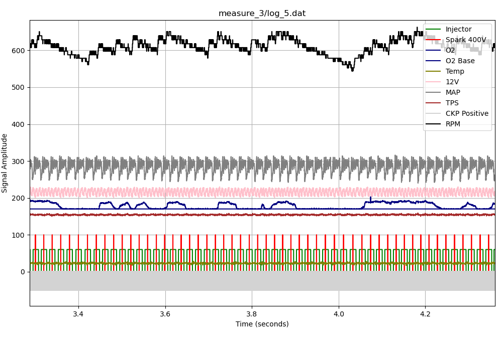
...and a zoomed in example:
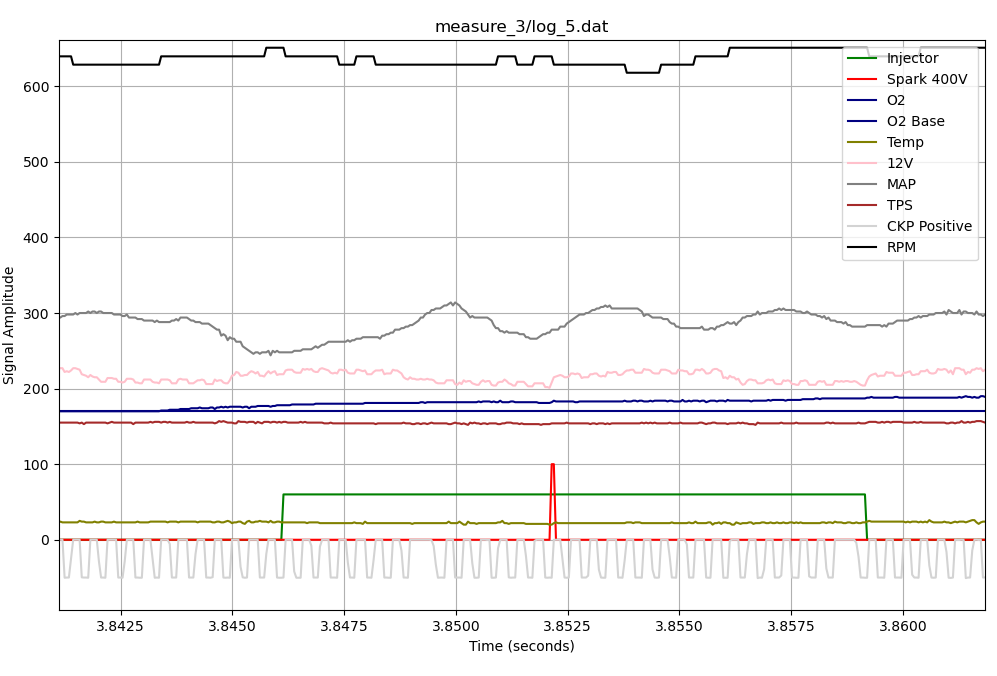
The chart displays the engine signals while trying to reach maximum RPM (full throttle). CKP pulses are intentionally inverted and go below zero line to prevent overlapping with the other signals. Red line is the spark signal, it is measured using discrete input so it's level means nothing, only the time of ECU-generated spark signal is measured (about 400V, goes directly to the coil). Green is the injector pulse, also discrete and its level should be ignored but the width of the pulse is important. Brown line is throttle position sensor, it is in its max position on the picture. Blue is the oxygen sensor, grey is MAP, pink is 12V power supply line of the vehicle. Olive is the engine temperature.
Black line is RPM and it is not measured but calculated using CKP pulses period, its is dawn divided by 10 for convenience. It looks noisy, this is because the sampling frequency is not enough to read original CKP form. But more than enough for visual analysis. Notice that every combustion event is visible on the RPM line, the moments it raises (rotation speed increase) after every spark. I assume not only the fact of success combustion may be seen here but also the quality of every single combustion and its stability. Impressive! And very helpful in the diagnostics.
The problem is depicted clearly: it is full throttle but cant accelerate higher than 6k RPM. What is interesting here is the oxygen sensor readings: it drops to zero (to the level of thin horizontal blue line) from time to time indicating lean mixture or a combustion problem. RPM line indicates the second: many combustion strokes (the moments after red spark pulses on the chart) are not followed by RPM increase meaning there was no combustion at all and the crankshaft decelerated. There could be many reasons for that like low fuel pressure or clogged injector but these were replaced recently and were out of suspect. What i could definitely say after the measurements that the electronic part of the vehicle worked well, fuel amount, timings etc... and There were no reasons left to postpone engine disassembly. The issue was fixed after valve replacement (it appeared that they had been running with tight clearance for some time and suffered permanent damage).
Well, the device was definitely worth building, at least for me. I was surprised by the clear and informative picture it provided about such a complex system. Especially the fact that every combustion event can be seen and analyzed! Just FYI, my vehicle doesn't provide much data via OBD2: only averaged oxygen readings, no MAP details at all, as well as no injection info. And of course, nothing about combustion/crankshaft acceleration! Even the check engine light was ignoring the obvious problem in vehicle performance.
ToDo
The development is not finished yet; I will keep updating the repository. In the nearest plans:
- the current SPI protocol implementation assumes the same sampling rate for all inputs, which is not optimal. Some signals change slowly (like temperature sensor or MAP) while others change faster (CKP). Implementing a dynamic SPI packet structure could lower the amount of data sent per second and thus allow for an increased sampling rate for the faster signals;
- flexible and configurable STM32 firmware that allows for covering many tasks without firmware updates;
- kernel-mode Linux module for RPI to work with the inputs and outputs in a standard way (e.g.,
echo "out5 1" > /dev/ctlpie); - configure RPI environment to update, build, and upload the firmware for STM32 (for on-the-go adjustments using an SSH connection from a tablet or phone).